preferable
夏琛15672845785…… [答案] adj.更好的,更合意的 例句: 1 He finds country life preferable to living in the city. 他感到在乡村生活比在城市生活要好些. 2 He finds country life preferable to that of living in the city. 他感到在乡村生活比在城市更好. 3 Cold food would be preferable in ...
@牟佳2690:PREFERABLE是什么意思? -
夏琛15672845785…… preferable adj. 更可取的, 更好的, 更优越的
@牟佳2690:preferable是什么意思 -
夏琛15672845785…… preferable [英][ˈprefrəbl][美][ˈprɛfərəbəl, ˈprɛfrə-] adj.更好的,更可取的; 略胜一筹的; 例句: 1. This is the classic and preferable model of reform. 这是经典的、更可取的改革模式. 2. A preferable solution today would be marine reserves, the more, and the bigger, thebetter. 如今一个更可取的措施是海洋保护区,保护区越多越大,效果越好
@牟佳2690:preferred,preferable有什么区别?举个例子, - 作业帮
夏琛15672845785…… [答案] preferred 它是个adj,意思是首选的 例:1.preferred above all others. 比其他事物先被选到的. 2.Common stock and preferred stock. 普通股、优先股 preferable 它是个adj,意思是更可取的,更好的,更优越的 例:1.M appears preferable to N. 看来m...
@牟佳2690:preferrable是什么意思 -
夏琛15672845785…… preferable 英[ˈprefrəbl] 美[ˈprɛfərəbəl, ˈprɛfrə-] adj. 更好的,更可取的; 略胜一筹的;
@牟佳2690:preferable是什么意思
夏琛15672845785…… 可选择的,可供挑选的
@牟佳2690:preferable偏爱的反义词加前缀吗,怎么加? -
夏琛15672845785…… preferable 英[ˈprefrəbl] 美[ˈprɛfərəbəl, ˈprɛfrə-] adj. 更好的,更可取的; 略胜一筹的; [例句]A big earthquake a long way off is preferable to a smaller one nearby 远处发生大地震总比在附近发生小地震好.
@牟佳2690:prefer和preference和preferable还有preferably怎么用? -
夏琛15672845785…… 注意单词词性 prefer 是动词 prefer-ance 是 动词加-ance变成的名词 preferable 是 动词加-able 编程的形容词 preferably是形容词加y 变成的副词 他们词性完全不一样 名词 只能做主宾补 动词 只能做谓语形容词 只能修饰名词 或做表语 做定语副词只能 修饰形容词 动词 副词 或全句做状语纯手打 希望给分
@牟佳2690:preferred,preferable有什么区别 -
夏琛15672845785…… 含意不同
- Narrow Pulse Width Laser Induced Reverse Selective Removal of Metal Thin Films to Fabricate Microcircuits (Invited)
- 崔佳琪, 谢小柱, 黄亚军, 李兆艳, 罗宇航, 龙江游
- 光子学报 2023年52卷第7期 文章编号:0752306
- 作者机构:
- 1.广东工业大学 物理与光电工程学院,广州 510006
- 2.广东工业大学 机电工程学院,激光微纳加工研究中心,广州 510006
- 3.广东工业大学 实验教学部,广州 510006
- DOI:10.3788/gzxb20235207.0752306 中图分类号:TG665
- 纸质出版日期:2023-07-25,
- 收稿日期:2023-04-10,
- 录用日期:2023-05-15
- 扫 描 看 全 文
- 引用本文
窄脉宽激光诱导背向选择性去除金属薄膜制备微电路(特邀)
崔佳琪 ; 谢小柱 ; 黄亚军 ; 李兆艳 ; 罗宇航 ; 龙江游 ;
PDF下载
HTML全文
图(10)表(1)
参考文献
出版信息
数据统计
论文导航
摘要
为了在透明基板上制备出导电性能良好的微电路,研究了窄脉宽激光正向和背向选择性去除金属薄膜制备的微结构形貌特征,开展了纳秒激光选择性去除Cu薄膜(厚度为150 nm)的实验和温度场仿真研究,揭示了正、背面去除的烧蚀机理和材料的喷射机制。实验结果表明,当激光脉冲能量为0.270~0.542 μJ,扫描速度为2 mm/s时,激光诱导背向去除金属薄膜在加工质量方面优于正向加工,其去除几何精度高,轮廓边缘平整,几乎没有溅射。采用优化后的纳秒激光加工工艺参数,激光脉冲能量为0.403 μJ, 扫描速度2 mm/s,扫描线间距为3 μm,制备出均匀分布的铜阵列图案。在相同参数下对玻璃基板上的铜薄膜背向选择性去除,得到具有良好导电性和粘附性的微电路。
Abstract
Nanosecond laser processing technology is widely used in Integrated Circuits (IC), optoelectronic devices, biology, medical, aerospace, and network technology due to its low cost, high precision, non-contact directional processing, and high efficiency. As the feature size of IC and Optoelectronics continues to decrease, copper (Cu) has become the mainstream interconnect material in electronic components, which has the advantages of low cost, low resistance, strong conductivity, high thermal conductivity and excellent ductility. Microcircuits prepared by narrow pulse laser induced selective ablation of Cu films on transparent substrates have attracted extensive attention from researchers because of their excellent optical and electrical properties. It has become a research hotspot in this field on how to obtain higher processing quality and efficiency, satisfy the processing requirements of various materials and structures. In recent years, the major processing method has been laser forward induced selective ablation of metal thin films to fabricate microstructures. However, this method inevitably produces heat-affected zones and nano-ripples during processing, this situation seriously reduces the quality and photoelectric properties of the metal film microstructure. In order to decrease the influence of laser thermal effect, avoid the accumulation of remelted material, and effectively improve the surface morphology and photoelectric properties of microstructure, this paper uses a narrow pulse width laser to selectively remove metal thin films and prepare microcircuits on the rear side. Firstly, the laser beam passes through the transparent substrate, and then irradiates the glass substrate and Cu film interface for laser selective induced ablation. Part of the Cu film in the ablation area is vaporized, and a huge pressure is generated in the closed space, thereby promoting the remaining metal film on the transparent substrate to be ejected. This unique ablation process has become an important preparation method for metal film microstructure owing to its high removal efficiency and high-quality processing effect. Based on the fabrication of microgrooves by nanosecond laser removing metal films, the effects of process parameters such as laser pulse energy and scanning speed on the front and rear side ablation of metal films by narrow pulse width laser (λ=532 nm, τ=1.8 ns) were investigated. By comparing the relationship between the groove width and the laser pulse energy at the same scanning speed, it can be concluded that the groove width increases with the enlargement of laser pulse energy on the front and rear side ablation. When the laser energy enlarges to a certain value, the groove width gradually reaches a certain level, and then remains stable. On the front side ablation, the width of the groove decreases with the increase of the scanning speed. At the same time, on the rear side ablation, the groove width is not sensitive to the scanning speed. As the scanning speed increases, the groove width does not change significantly. Since the width of the groove in the reverse removal is independent of the laser scanning speed, the edge shape of the groove can be improved by changing the laser scanning speed. By further optimizing the process parameters and analyzing the surface morphology of the microstructure in detail, it is proved that the performance of the microgrooves prepared by narrow pulse width laser (E=0.403 μJ, v=2 mm/s) on the rear side ablation is better than the front side. It not only has a straight and steep edge morphology, but has almost no sputtering on the edge. Through the experiments comparison of the front and reverse removal, it can be seen that the groove removed by the laser from the rear side is narrower than that removed from the front, which is impertinence of the variation of laser power. The difference in groove width between the two laser induced ablation methods could be attributed to diverse beam propagation and material removal processes. In addition, the 3D morphology of the microgrooves is characterized by a Confocal Laser Scan Microscope (CLSM), and the removal depth of the microgrooves is about 150 nm. This indicates that the Cu film on the glass substrate is completely removed and the glass substrate is not damaged which is crucial for the electronic isolation and photoelectric properties of actual electronic devices. In consequence, under the existing experimental conditions of our group, the microstructure of metal film prepared on rear side ablation has preferable quality. Combined with the temperature field simulation results of metal film by narrow pulse laser selective removal, the ablation mechanism and material removal mechanism of front and rear side ablation are revealed from the perspective of experiment and theory. To verify the feasibility of this removal method, uniformly distributed Cu arrays and complex microcircuit patterns are prepared when the laser energy is set to 0.403 μJ, and the scanning speed is 2 mm/s. The resistivity of the microcircuit measured by the double probe measuring instrument is 1.81 μΩ·cm, which is equivalence with the resistivity of the copper body. As a result, the microcircuit has excellent conductivity. Finally, the sample is placed in deionized water for ultrasonic 10 min, and the morphology of the microcircuit has no change. It proves the microcircuit processed by laser reverse processing has good adhesion and could be used for IC. Furthermore, this method has good application prospects.
译
关键词
窄脉宽激光; 背面去除; 温度场仿真; 金属薄膜; 微电路
Keywords
Narrow pulse width laser; Reverse removal; Temperature field simulation; Mental thin film; Microcircuit
译
OCIS码
140.3538; 310.3915; 310.6845; 350.3390; 250.3140
0 引言
近年来,激光加工技术在集成电路、光电子器件、半导体器件以及医疗航天等领域扮演着越来越重要的角色[1-4]。利用激光选择性诱导金属薄膜制备微结构在工业、国防、通信、医疗等领域应用广泛,如电路板和光电设备的制造、微电子系统和太阳能电池的制备[5-7]。如何获得更高的加工质量和加工效率,并满足各种材料或结构的加工需求成为该领域的研究热点。目前,在透明基板上制备微电路的方法主要包括:激光诱导选择性去除金属薄膜、激光刻蚀工艺、紫外光刻、电子束光刻、激光诱导还原烧结以及直接墨水书写等方法。然而刻蚀工艺、光刻技术以及墨水直写等方法存在工艺复杂、缺乏工艺灵活性、制备的微电路电阻率高、粘附性较差、会造成环境污染等问题[8-12]。近年来制备微电路的主流方法是激光正向选择性烧蚀金属薄膜,例如:PAENG D等[13, 14]通过纳秒激光正向选择性去除铜薄膜制备出柔性透明导电电极;LEMKE A等[15]使用皮秒激光正向选择性去除铜铟镓硒(CIGS)薄膜制备太阳能电池功能层;ULMEANU M等[16]利用飞秒激光对钴(Co,20 nm)/铜(Cu,6 nm)/钴(Co,3 nm)三层复合薄膜结构进行了选择性去除和图案化。然而一些研究学者发现在激光正向诱导金属薄膜的过程中不可避免会产生热影响区、死区或者是纳米波纹,并且形成的重熔物常隆起在凹槽的边缘处,这种情况会严重降低凹槽的质量并且影响到光电特性[7, 14, 17-22]。所以,激光背面选择性烧蚀的方法受到了越来越多学者的关注,即激光束首先穿过透明基板,然后照射到薄膜上进行选择性诱导烧蚀。背面烧蚀金属薄膜和正面烧蚀的作用机理虽然相同,但是材料的喷射机制存在明显的差异,背面去除是通过部分金属薄膜气化,在密闭空间产生的压强推动剩余金属薄膜从透明基板上喷射出去[23, 24]。因此这种去除方式能够减小热影响区的影响,避免重熔物的堆积,有效提高金属微结构的质量和光电性能。除了用于激光诱导前向转移工艺之外,这种独特的烧蚀工艺已成为一种新型的金属薄膜微结构的制备方法。一些学者已经证明了背面烧蚀的去除效率比正面烧蚀过程高一个甚至两个数量级[5]。由此证明了背面烧蚀是一种高效、高质量的薄膜结构化烧蚀方法,在金属薄膜选择性结构的制备中发挥着越来越大的作用。
本文以窄脉宽激光去除金属薄膜制备微槽为基础,研究了激光脉冲能量以及扫描速度等工艺参数对正向和背向选择性去除金属薄膜的影响,详细分析了微槽的表面形貌,结合窄脉宽激光选择性去除金属薄膜的温度场仿真结果,从实验和理论的角度揭示正、背面去除的烧蚀机理和材料的去除机制。在此基础上,制备出具有高表面质量的Cu阵列图案以及良好导电性的复杂微电路。
1 实验装置与方法
图1(a)显示了实验装置的示意图。使用波长为532 nm,脉冲重复频率为1 kHz,脉冲持续时间为1.8 ns,最大输出能量为1 μJ的MAC系列微片激光器(MCA-1-8-50,Real Light)作为激光源。激光功率和偏振状态由λ/2波片和偏振立方分束器(Polarization Beam Splitter,PBS)控制。4×扩束镜用于将激光束从2 mm扩展到8 mm(1/e2)。激光束经过偏振和扩束,并通过两个平面镜引导到二向色镜。最后,窄脉宽激光通过一个20倍显微镜物镜(M Plan APO 20,NA=0.42)聚焦在样品上,根据公式ω0=0.61 λ/NA计算出高斯光束聚焦点的半径约为0.773 μm,其中λ代表激光的波长,NA代表数值孔径。
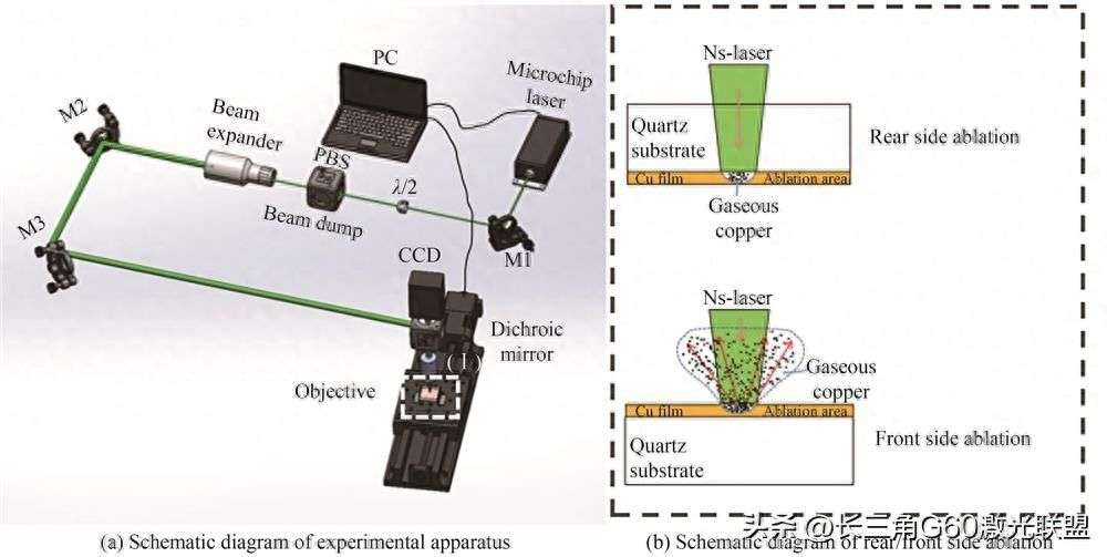
图1 实验装置系统以及正背面烧蚀铜薄膜示意图
Fig.1 Schematic diagram of experimental apparatus and the rear and front side ablation of Cu film
下载: 原图 | 高精图 | 低精图
样品由1 mm厚的紫外级石英玻璃(型号为JGS1)和通过磁控溅射制备的铜薄膜(厚度为150 nm)组成,并且使用手动三轴台的定制夹具将样品固定在实验平台上面。通过调整Z轴平台和同轴CCD相机,焦点被精确地设置在玻璃基板—铜薄膜的界面上。实验过程通过CCD同轴摄像机进行实时监控。
2 实验结果与讨论
2.1 激光能量和扫描速度对正、背面烧蚀金属薄膜的影响
图2显示了激光脉冲能量分别为0.072 μJ、0.155 μJ、0.27 μJ、0.403 μJ和0.542 μJ时,正面和背面烧蚀微沟槽的宽度随着扫描速度的变化。通过对比同一扫描速度下凹槽宽度与激光脉冲能量的关系,可以得出正面和背面去除时凹槽宽度随着激光脉冲能量的增大而增大。当激光能量增大到一定值时,凹槽宽度逐渐达到一定水平,之后保持稳定。对于正面烧蚀,凹槽的宽度随着扫描速度的增加而减小;而背面烧蚀时,凹槽宽度对扫描速度不敏感,随着扫描速度的增大,凹槽宽度无明显变化。这种现象是由不同的材料去除机制引起的。在正面烧蚀过程中,材料去除是由蒸发气化引起的,而背面烧蚀中,Cu薄膜的蒸发气化首先发生在Cu薄膜和玻璃基板之间的封闭空间,随着压力的增大,Cu薄膜膨胀进而被剥离,导致Cu薄膜的去除,因此凹槽宽度对背面烧蚀中激光的扫描速度不敏感[5, 25]。由于背面去除中凹槽宽度与激光扫描速度无关,可以通过改变激光扫描速度改善凹槽的边缘形态,进一步优化参数。
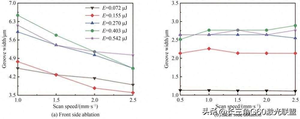
图2 纳秒激光高斯光束在0.5~2.5 mm/s扫描速度和0.072~0.542 μJ脉冲能量下烧蚀的微凹槽宽度
Fig.2 The widths of micro-grooves ablated by ns laser Gaussian beam at the scan speed from 0.5 to 2.5 mm/s and pulse energy from 0.072 to 0.542 µJ
下载: 原图 | 高精图 | 低精图
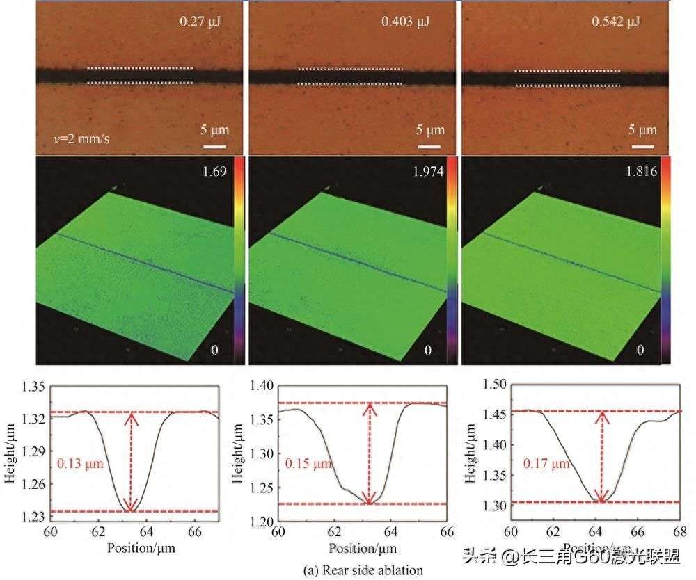
从图3可以看到激光从玻璃基板照射金属薄膜去除的凹槽比从正面照射去除的凹槽窄,这与激光功率的变化无关,两种激光烧蚀方法之间的凹槽宽度差异可归因于不同的光束传播和材料去除过程。在正面烧蚀中,激光束照射在Cu薄膜的表面,沿着激光的扫描轨迹,Cu薄膜蒸发形成微槽。在背面烧蚀中,Cu薄膜发生非线性吸收过程。开始时,只有靠近玻璃的薄层Cu被烧蚀,并且由于Cu的气化,在Cu薄膜层和玻璃基板之间的密闭空间形成高压。然后,随着脉冲数量的增加,压力增加,Cu薄膜的外层最终将完全剥离[1, 5, 26]。根据实验结果,背面烧蚀应该是在Cu薄膜图案化过程中获得更窄凹槽的去除方法。
下载: 原图 | 高精图 | 低精图

下载: 原图 | 高精图 | 低精图
图3 相同条件下2 mm/s扫描速度、不同脉冲能量下的正背面去除对比
Fig.3 Comparison diagram of front and rear ablation under the same conditions at the scan speed 2 mm/s and different pulse energy
除了可以得到更窄的凹槽,背面去除制备的凹槽边缘线与正面去除相比更平整、溅射物较少,并且边缘没有熔融物的堆积,如图4所示。这是由于背面烧蚀时,激光辐射通过透明基板传输,并在金属薄膜和基板之间的界面处被吸收。铜在绿光波段的激光辐射光学穿透深度小于铜薄膜的厚度,由于空间封闭所以蒸发的材料不能直接喷射,引起压力增加,从而导致剩余金属薄膜膨胀。如果蒸发材料的压力超过铜薄膜的拉伸应力,则剩余金属薄膜被剪切掉并冲出完整的金属盘[26]。在这种烧蚀机制中,不会发生诸如熔体残留物之类的热效应。
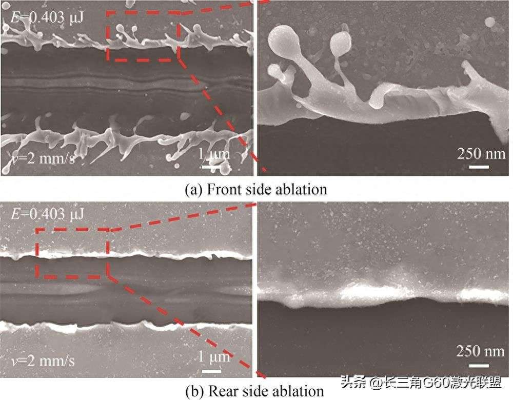
图4 正、背面去除的SEM图像
Fig.4 SEM image of the front and rear side ablation
下载: 原图 | 高精图 | 低精图
此外,激光脉冲能量为0.403 μJ时,烧蚀区域的深度约为150 nm,正好等于Cu薄膜的厚度。这表明玻璃基板上的Cu薄膜被完全去除且玻璃基板没有损伤。这对于实际电子器件的电子隔离和光电性能至关重要。因此,在本课题组现有的实验条件下,背面烧蚀制备的金属薄膜微结构具有更好的质量。
2.2 窄脉宽激光正背面烧蚀金属薄膜的温度场仿真
为研究纳秒激光正背面选择性去除金属薄膜的烧蚀机制以及材料的喷射过程,采用有限元法对激光正向和背向辐照金属薄膜的局部温度场进行了模拟计算。考虑到激光能量分布以及几何模型的轴对称特点,选用二维轴对称模型进行仿真计算。构建仿真模型时采用面热源模拟激光脉冲的热效应,根据激光器参数选择高斯分布的热源模型,即采用高斯函数来描述光斑上热流密度。
q(r)=3ηEτπd2exp (−3r2d2)��=3���π�2exp -3�2�2 | (1) |
式中,q(r)为距离光斑中心r处的热流密度,η为激光的吸收系数,由于铜薄膜在室温条件下被532 nm激光辐照,所以η=0.38,E为激光脉冲能量,τ为激光脉宽,取1.8 ns,d为激光光斑半径,取0.773 µm。
温度场模型的控制方程为
C∂T∂t=∇⋅(k∇T)+H�∂�∂�=∇·�∇�+� | (2) |
式中,C为材料比热容,T为材料温度,t为时间,k为热导率,H为热源项,设置初始条件为T=293.15 K。由于激光脉冲的作用时间极短,忽略铜薄膜与约束层的热传导,所有边界均采用热对流边界条件为
∇⋅(k∇T)−q+h(T−T0)+σε(T4−T40)=0,(x,y)∈H,t>0∇·�∇�-�+ℎ�-�0+���4-�04=0,�,�∈�,�>0 | (3) |
式中,h为对流换热系数,σ为斯蒂芬-玻尔兹曼常数,ε为工件辐射率,T0为环境温度,取为室温300 K。由于铜薄膜会产生相变,计算过程中需要考虑相变所需要的熔化和汽化潜热,具体参数见表1。
表1 铜的热物理特性参数
Table 1 Thermo-physical properties of copper
Parameters | Values |
Latent heat of fusion/(J·g-1) | 206.5 |
Melting point/K | 1357 |
Latent heat of vaporization(J·g-1) | 4 724.5 |
Boiling point/K | 2 840 |
Reflectivity | 0.87 |
下载: 导出CSV
通过参数和计算公式,利用COMSOL软件仿真出激光正面和背面烧蚀的温度场。图5为激光脉冲能量为0.083 μJ时,窄脉宽纳秒激光正向和背向选择性烧蚀Cu薄膜的情况下,Cu薄膜表面温度随激光辐照时间的变化。从图中可以看出激光脉冲能量为0.083 μJ时,已经达到正面烧蚀的气化温度,正面烧蚀的Cu薄膜开始气化;而背面烧蚀的Cu薄膜还未达到气化温度。这是因为背面去除的过程中,激光束首先穿过基板,然后在基板-薄膜界面处照射位于透明基板上的金属薄膜,在此过程中玻璃基板会吸收部分能量造成能量的损失。
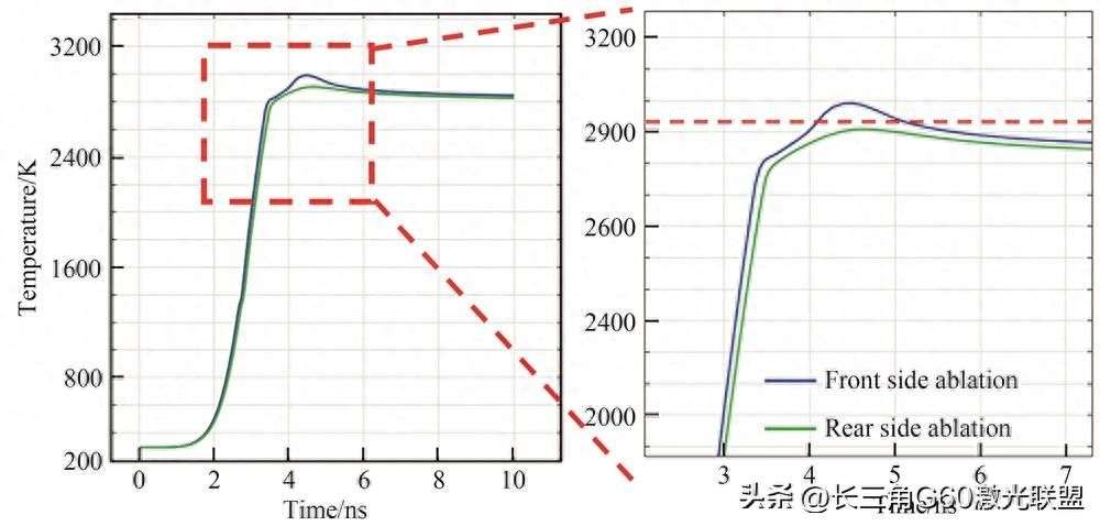
图5 脉冲能量为0.083 μJ时,正背面烧蚀Cu薄膜的仿真温度场
Fig.5 Simulated temperature field of ablation Cu film on the front and rear side at a pulse energy of 0.083 μJ
下载: 原图 | 高精图 | 低精图
为了验证仿真模型的可靠性,设定脉冲能量分别为0.072 μJ(小于0.083 μJ)和0.155 μJ(大于0.083 μJ),使用单脉冲能量正背面烧蚀Cu薄膜,利用光学显微镜和激光共聚焦显微镜观察烧蚀坑的表面形貌。图6为脉冲能量为0.072 μJ和0.155 μJ时,使用单脉冲能量正背面烧蚀Cu薄膜的表面形貌。从图6(a)(c)和(e)(g)中可以看出当脉冲能量小于0.083 μJ时,正面烧蚀(图6(a))的Cu薄膜处于熔融状态,有重熔物的堆积;而背面烧蚀(图6(e))的Cu薄膜未达到沸点,无重熔物的堆积。上述结果与图5中温度场的仿真结果相对应,这是由于激光的入射方向不同,从而导致背面入射的激光束能量在穿过玻璃基板过程中产生衰减。随着脉冲能量增大至0.155 μJ,此时的激光束能量远大于Cu薄膜的气化温度。从图6(b)(d)和(f)(h)可以看到正背面烧蚀均发生气化蒸发,从图6(b)看出正面去除的凹坑边缘有重熔物的堆积,边缘有部分凸起,而图6(f)背面去除的凹坑边缘平整,无重熔物的堆积,这是由于正背面去除的材料喷射机制不同造成的。
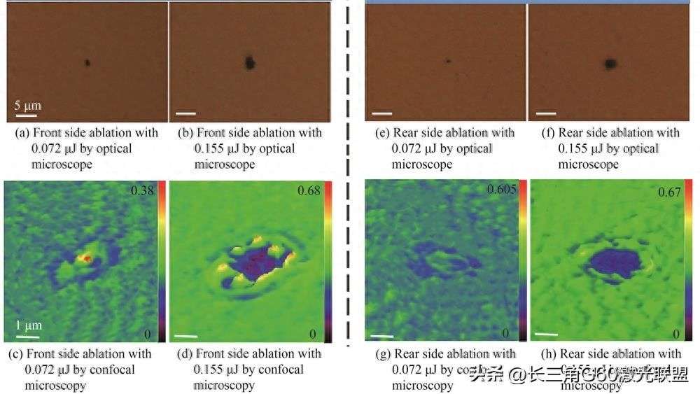
图6 脉冲能量为0.072 μJ和0.155 μJ时,正背面单脉冲烧蚀Cu薄膜的表面形貌
Fig.6 The surface morphology of Cu film by the single pulse on the front and rear side ablation at the pulse energy of 0.072 μJ and 0.155 μJ
下载: 原图 | 高精图 | 低精图
当激光辐照时间为3.9 ns时,激光透过玻璃基板照射至玻璃基板-铜薄膜处,靠近玻璃基板处的Cu薄膜达到沸点,该温度足以使Cu薄膜被烧蚀气化,但是处于封闭空间不能直接喷射,随着激光辐照时间的增加,气化区域压力增加,导致剩余熔化的金属薄膜膨胀。当金属薄膜膨胀的压力大于铜薄膜的拉伸应力时,剩余金属薄膜会被剪切掉喷射出去,从而在背面烧蚀中,不会发生边缘残留物等热效应,制备的金属薄膜微结构具有更好的质量,如图7(a)所示。而正面烧蚀的过程中,激光直接烧蚀铜薄膜表面,当辐照时间为3.9 ns时,Cu薄膜表面被激光辐照的区域发生蒸发,而激光光斑边缘处的区域还未达到沸点,处于熔融状态呈液态,剩余区域还未达到熔点处于固态铜,如图7(b)所示。沿着激光扫描方向,Cu薄膜蒸发形成微凹槽,但是在激光扫描的过程中会导致激光辐照边缘熔化的Cu在凹槽两侧形成重熔物,堆积在凹槽边缘处。不仅会导致较多的溅射物,而且影响凹槽两侧陡峭边缘的形成,严重影响微结构的表面形貌和质量。
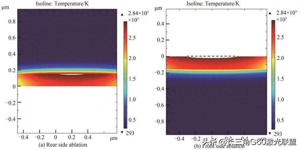
图7 烧蚀时间为3.9 ns时,纳秒激光烧蚀Cu薄膜的仿真温度场
Fig.7 Simulated temperature field of ablation Cu film on the front and rear side at 3.9 ns
下载: 原图 | 高精图 | 低精图
2.3 激光背向选择性去除Cu薄膜制备微电路
由于具有出色的光学和电学性能,在透明基板上制备金属微电路广泛应用于光电子、太阳能电池等领域,具有良好的应用前景。经过上述实验和仿真计算,证明了背面烧蚀优于正面烧蚀,并且利用窄脉宽激光背面选择性去除铜薄膜制备出边缘笔直陡峭、几乎无溅射以及去除干净的微凹槽。为了验证上述金属化方法的可行性,使用优化后的参数在玻璃基板上背向选择性去除Cu薄膜制备出均匀分布的阵列图案(如图8所示)以及复杂的微电路图案(如图9所示)。
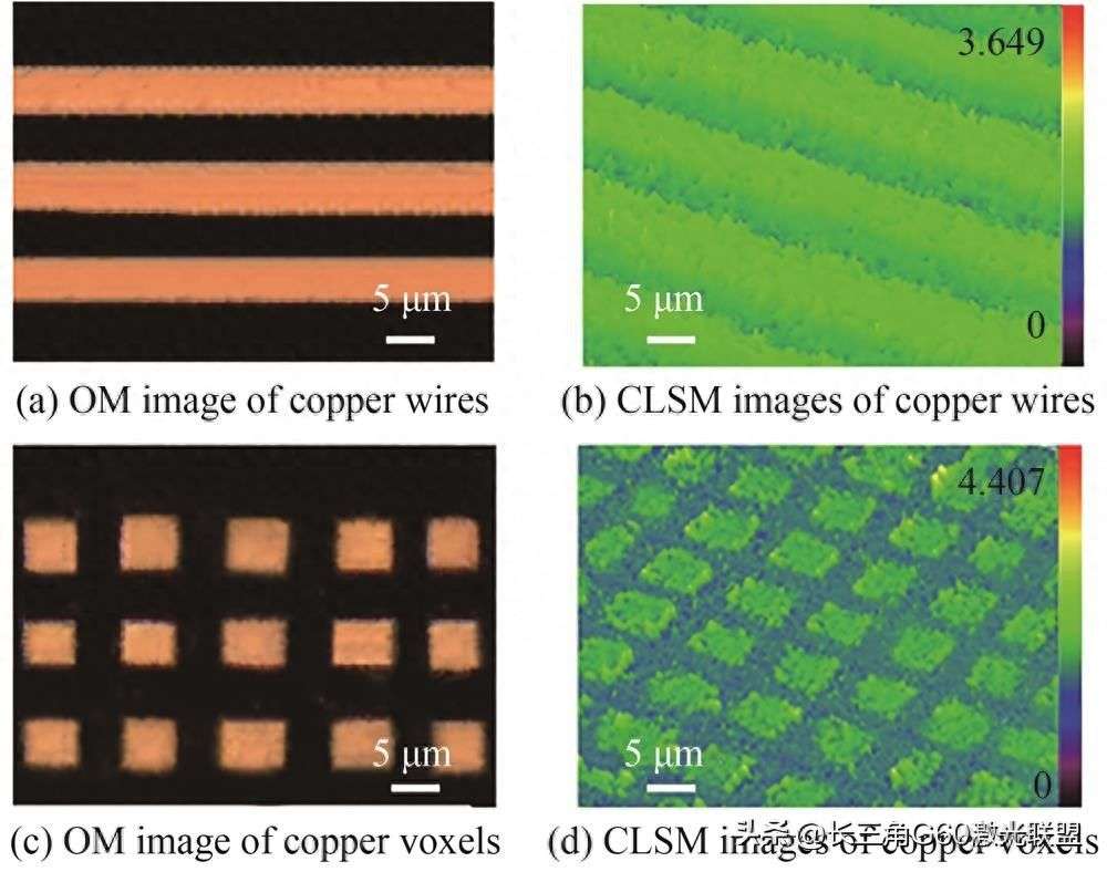
图8 激光背面去除制备Cu阵列
Fig.8 Cu array are prepared by laser induced rear side ablation
下载: 原图 | 高精图 | 低精图
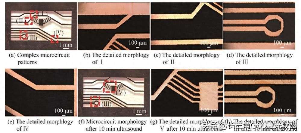
图9 激光背向选择性去除制备复杂微电路
Fig.9 Complex microcircuits are prepared by laser induced rear side selective ablation
下载: 原图 | 高精图 | 低精图
由背面去除制备微凹槽的实验可以得知,背面去除过程中激光扫描速度对凹槽宽度无明显影响,通过调节扫描速度进一步优化参数,可以有效提高微结构的3D形貌和质量。通过实验发现,当激光脉冲能量为0.403 μJ,扫描速度为2 mm/s,扫描线间距为3 μm时,窄脉宽激光背面选择性烧蚀制备的铜阵列表面形貌良好,如图8所示。从图8(a)光学显微镜图像和(b)共聚焦图像中,可以看出制备的铜线线宽均匀、边缘陡峭笔直、溅射物较少,具有良好的形貌。利用激光横向和纵向交叉扫描制备出Cu体素阵列,从图8(c)、(d)可以看出Cu网格边缘平整,几乎无溅射物残留。
透明基板上制备铜薄膜微电路既满足了石英基板的高透光率和低成本的要求,又保留了铜薄膜的高导电性、高导热性和良好的延展性,具备良好的光电特性。当激光脉冲能量为0.403 μJ,扫描速度为2 mm/s时,使用窄脉宽激光背向选择性去除铜薄膜制备出复杂的微电路图案,如图9(a)~(h)所示。从导电性的角度来看,使用双探针测量仪测量微电路计算电阻率。电阻率根据等式ρ=(R·S)/L计算,其中ρ是电阻材料的电阻率(μΩ·cm);I是电阻的长度(cm);S是电阻的横截面积(cm2),它是从微电路的横截面轮廓计算出来的;R是电阻(μΩ),由双探针测量仪直接测得。计算得出铜微电路的电阻率为1.81 μΩ·cm,微电路电阻率约为铜体的电阻率(约1.76 μΩ·cm),微电路具有良好的导电性能。然后将微电路样品放入去离子水中超声处理10 min后,微电路的表面形态没有变化,如图9(f)~(h)。
3 结论
本文采用532 nm、1.8 ns的激光选择性去除透明基板上的金属薄膜,通过光学显微镜、激光共聚焦显微镜以及扫描电子显微镜对金属薄膜微结构去除深度和表面形貌进行了表征。研究了激光正向和背向选择性去除中脉冲能量、扫描速度等工艺参数对去除效果的影响规律,并且采用有限元法对Cu薄膜表面的温度场和相变过程进行了仿真计算,揭示了正背面去除的烧蚀机制以及材料的喷射机制。实验结果表明,在窄脉宽激光的诱导下背面选择性烧蚀金属薄膜制备的微结构明显优于正面烧蚀,几乎没有溅射物,边缘平整度更好并且制备的微结构尺寸更小。最终设置纳秒激光单脉冲能量为0.403 μJ,扫描速度为2 mm/s,扫描线间距为3 μm,制备出均匀分布的铜阵列图案,进一步对玻璃基板上的铜薄膜选择性去除从而得到导电性能、粘附性良好的微电路。
来自:光子学报
长三角G60激光联盟陈长军转载
","gnid":"98f1ce782c4be3257","img_data":[{"flag":2,"img":[{"desc":"","height":"503","title":"","url":"http://p1.img.360kuai.com/dmfd/__60/t01b4dfd1c2b90c9a12.jpg","width":"1000"},{"desc":"","height":"398","title":"","url":"http://p1.img.360kuai.com/dmfd/__60/t011ed55c232a6308f4.jpg","width":"1000"},{"desc":"","height":"834","title":"","url":"http://p0.img.360kuai.com/dmfd/__60/t01a65ad8bf8b4db0e5.jpg","width":"1000"},{"desc":"","height":"852","title":"","url":"http://p2.img.360kuai.com/dmfd/__60/t010bd42efd89e62dc7.jpg","width":"1000"},{"desc":"","height":"780","title":"","url":"http://p0.img.360kuai.com/dmfd/__60/t01a8f05db03616d004.jpg","width":"1000"},{"desc":"","height":"478","title":"","url":"http://p1.img.360kuai.com/dmfd/__60/t0161354328006e3939.jpg","width":"1000"},{"desc":"","height":"563","title":"","url":"http://p0.img.360kuai.com/dmfd/__60/t018b118d1a6cbb29e9.jpg","width":"1000"},{"desc":"","height":"498","title":"","url":"http://p0.img.360kuai.com/dmfd/__60/t01727f06ec9a5e76a0.jpg","width":"1000"},{"desc":"","height":"788","title":"","url":"http://p2.img.360kuai.com/dmfd/__60/t0194d695288a4b98b5.jpg","width":"1000"},{"desc":"","height":"444","title":"","url":"http://p2.img.360kuai.com/dmfd/__60/t0183f0d2865f040a83.jpg","width":"1000"}]}],"original":0,"pat":"art_src_3,sexf,sex4,sexc,fts0,sts0","powerby":"pika","pub_time":1694248920000,"pure":"","rawurl":"http://zm.news.so.com/f64ab123677bc79adaa2528bf5b350da","redirect":0,"rptid":"02e1c5eb2b8eb522","rss_ext":[],"s":"t","src":"江苏激光产业创新联盟","tag":[],"title":"窄脉宽激光诱导背向选择性去除金属薄膜制备微电路